Classification of Materials:
- The classification of solids into insulators, metals, and semiconductors can be explained with the help of the energy band diagram.
Insulators:
- The valence band and the conduction band are separated by a large energy gap.
- The forbidden energy gap is approximately 6 eV in insulators.
- The gap is very large that electrons from valence band cannot move into conduction band even on the application of strong external electric field or the increase in temperature.
- Therefore, the electrical conduction is not possible as the free electrons are almost nil and hence these materials are called insulators.
- Its resistivity is in the range of 1011–1019 Ωm.
Conductors:
- In condutors, the valence band and conduction band overlap.
- Hence, electrons can move freely into the conduction band which results in a large number of free electrons in the conduction band.
- Therefore, conduction becomes possible even at low temperatures.
- The application of electric field provides sufficient energy to the electrons to drift in a particular direction to constitute a current.
- For condutors, the resistivity value lies between 10–2 and 10–8 Ωm.
Semiconductors:
- In semiconductors, there exists a narrow forbidden energy gap (Eg < 3eV) between the valence band and the conduction band.
- At a finite temperature, thermal agitations in the solid can break the covalent bond between the atoms (covalent bond is formed due to the sharing of electrons to attain stable electronic configuration).
- This releases some electrons from valence band to conduction band.
- Since free electrons are small in number, the conductivity of the semiconductors is not as high as that of the conductors.
- The resistivity value of semiconductors is from 10–5 to 106 Ωm.
- When the temperature is increased further, more number of electrons is promoted to the conduction band and increases the conduction.
- Thus, we can say that the electrical conduction increases with the increase in temperature.
- In other words, resistance decreases with increase in temperature.
- Hence, semiconductors are said to have negative temperature coefficient of resistance.
- The most important elemental semiconductor materials are Silicon (Si) and Germanium (Ge).
- The forbidden energy gaps for Si and Ge at at room temperature are 1.1 eV and 0.7 eV respectively.
Types of Semiconductors:
Intrinsic semiconductors:
- A semiconductor in its pure form without impurity is called an intrinsic semiconductor.
- Here, impurity means any other atom in the crystal lattice.
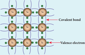
- Each Silicon atom has four electrons in the outermost orbit and is covalently bonded with the neighbouring atoms to form the lattice.
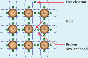
- A small increase in temperature is sufficient enough to break some of the covalent bonds and release the electrons free from the lattice.
- As a result, some states in the valence band become empty and the same number of states in the conduction band will be occupied.
- The vacancies produced in the valence band are called holes.
- As the holes are deficiency of electrons, they are treated to possess positive charges.
- Hence, electrons and holes are the two charge carriers in semiconductors.
- In intrinsic semiconductors, the number of electrons in the conduction band is equal to the number of holes in the valence band.
- The conduction is due to the electrons in the conduction band and holes in the valence band.
- These currents are represented as Ie and Ih
- The total current (I) is always the sum of the electron current (Ie) and the hole current ( Ih ) . I = Ie + Ih
- An intrinsic semiconductor behaves like an insulator at 0 K.
- The increase in temperature increases the number of charge carriers (electrons and holes).
- The schematic diagram of the intrinsic semiconductor in band diagram.
- The intrinsic carrier concentration is the number electron in the conduction band or the number of holes in the valence band in an intrinsic semiconductor.
Extrinsic semiconductors:
- The carrier concentration in an intrinsic semiconductor is not sufficient enough to develop efficient electronic devices.
- Another way of increasing the carrier concentration in an intrinsic semiconductor is by adding impurity atoms.
- The process of adding impurities to the intrinsic semiconductor is called doping.
- It increases the concentration of charge carriers (electrons and holes) in the semiconductor and in turn, its electrical conductivity.
- The impurity atoms are called dopants and its order is approximately 100 ppm (parts per million).
n-type semiconductor:
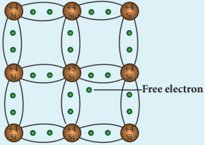
- A n-type semiconductor is obtained by doping a pure Germanium (or Silicon) crystal with a dopant from group V pentavalent elements like Phosphorus, Arsenic, and Antimony.
- The dopant has five valence electrons while the Germanium atom has four valence electrons.
- During the process of doping, a few of the Germanium atoms are replaced by the group V dopants.
- Four of the five valence electrons of the impurity atom are bound with the 4 valence electrons of the neighbouring replaced Germanium atom.
- The fifth valence electron of the impurity atom will be loosely attached with the nucleus as it has not formed the covalent bond.
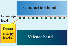
- The energy level of the loosely attached fifth electron from the dopant is found just below the conduction band edge and is called the donor energy level.
- At room temperature, these electrons can easily move to the conduction band with the absorption of thermal energy.
- Besides, an external electric field also can set free the loosely bound electrons and lead to conduction.
- It is important to note that the energy required for an electron to jump from the valence band to the conduction band ( Eg) in an intrinsic semiconductor is 0.7 eV for Ge and 1.1 eV for Si, while the energy required to set free a donor electron is only 0.01 eV for Ge and 0.05 eV for Si.
- The group V pentavalent impurity atoms donate electrons to the conduction band and are called donor impurities.
- Therefore, each impurity atom provides one extra electron to the conduction band in addition to the thermally generated electrons.
- These thermally generated electrons leave holes in valence band.
- Hence, the majority carriers of current in an n-type semiconductor are electrons and the minority carriers are holes.
- Such a semiconductor doped with a pentavalent impurity is called an n-type semiconductor.
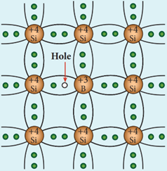
p-type semiconductor:
- Here, a trivalent atom from group III elements such as Boron, Aluminium, Gallium and Indium is added to the Germanium or Silicon substrate.
- The dopant with three valence electrons are bound with the neighbouring Germanium atom.
- As Germanium atom has four valence electrons, one electron position of the dopant in the Germanium crystal lattice will remain vacant.
- The missing electron position in the covalent bond is denoted as a hole.
- To make complete covalent bonding with all four neighbouring atoms, the dopant is in need of one more electron.
- These dopants can accept electrons from the neighbouring atoms.
- Therefore, this impurity is called an acceptor impurity.
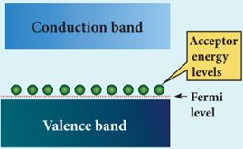
- The energy level of the hole created by each impurity atom is just above the valence band and is called the acceptor energy level.
- For each acceptor atom, there will be a hole in the valence band in addition to the thermally generated holes.
- In such an extrinsic semiconductor, holes are the majority carriers and thermally generated electrons are minority carriers.
- The semiconductor thus formed is called a p-type semiconductor.
DIODES:
P-N Junction formation:
Formation of depletion layer:
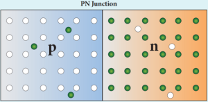
- A p-n junction is formed by joining n-type and p-type semiconductor materials.
- Since the n-region has a high electron concentration and the p-region a high whole concentration, electrons diffuse from the n-side to the p-side.
- This causes diffusion current which exists due to the concentration difference of electrons.
- The electrons diffusing into the p-region may occupy holes in that region and make it negative.
- The holes left behind by these electrons in the n-side are equivalent to the diffusion of holes from the p-side to the n-side.
- If the electrons and holes were not charged, this diffusion process would continue until the concentration of electrons and holes on the two sides were the same, as happens if two gasses come into contact with each other.
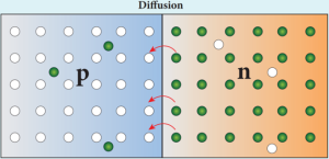
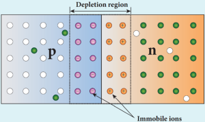
- But, in a p-n junction, when the electrons and holes move to the other side of the junction, they leave behind exposed charges on dopant atom sites, which are fixed in the crystal lattice and are unable to move.
- On the n-side, positive ion cores are exposed and on the p- side, negative ion cores are exposed.
- An electric field E forms between the positive ion cores in the n-type material and negative ion cores in the p-type material.
- The electric field sweeps free carriers out of this region and hence it is called depletion region as it is depleted of free carriers.
- A barrier potential Vb due to the electric field E is formed at the junction.
- As this diffusion of charge carriers from both sides continues, the negative ions form a layer of negative space charge region along the p-side.
- Similarly, a positive space charge region is formed by positive ions on the n-side.
- The positive space charge region attracts electrons from p-side to n-side and the negative space charge region attracts holes from n-side to p-side.
- This moment of carriers happen in this region due to the formed electric field and it constitutes a current called drift current.
- The diffusion current and drift current flow in the opposite direction and at one instant they both become equal. Thus, a p-n junction is formed.
Junction potential or barrier potential:
- The recombination of charge carriers takes place only to a certain point beyond which the depletion layer acts like a barrier to further diffusion of free charges across the junction.
- This is due to the fact that the immobile ions on both sides establish an electric potential difference across the junction.
- Therefore, an electron trying to diffuse into the interior of the depletion region encounters a negative wall of ions repelling it backwards.
- If the free electron has enough energy, it can break through the wall and enter into the p-region, where it can recombine with a hole and create another negative ion.
- The strength of the electric potential difference across the depletion region keeps increasing with the crossing of each electron until equilibrium is reached; at this point, the internal repulsion of the depletion layer stops further diffusion of free electrons across the junction.
- This difference in potential across the depletion layer is called the barrier potential. At 25 0 C, this barrier potential approximately equals 0.7 V for Silicon and 0.3 V for Germanium.
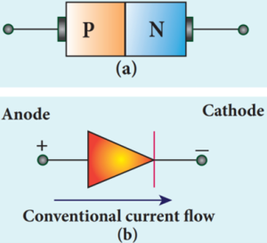
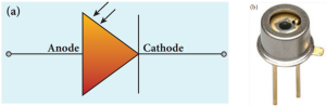
P-N Junction Diode:
- A p-n junction diode is formed when a p-type semiconductor is fused with an-type semiconductor.
- It is a device with single p-n junction.
Biasing a diode:
- Biasing means providing external energy to charge carriers to overcome the barrier potential and make them move in a particular direction.
- The charge carriers can either move towards the junction or away from the junction.
- The external voltage applied to the p-n junction is called bias voltage.
- Depending on the polarity of the external source to the p-n junction we have two types of biasing
- Forward bias
- Reverse bias
Forward Bias:
- If the positive terminal of the external voltage source is connected to the p-side and the negative terminal to the n-side, it is called forward biased.
- The application of a forward bias potential makes the electrons move into the n-side and the holes into the p-side.
- This initiates the recombination with the ions near the junction which in turn reduces the width of the depletion region and hence the barrier potential.
- The electron from the n-side is now accelerated towards the p-side as it experiences a reduced barrier potential at the junction.
- In addition, the accelerated electrons experience a strong attraction by the positive potential applied to the p-side.
- This results in the movement of electrons towards the p-side and in turn, holes towards the n-side.
- When the applied voltage is increased, the width of the depletion region and hence the barrier potential are further reduced.
- This results in a large number of electrons passing through the junction resulting in an exponential rise in current through the junction.
Reverse Bias:
- If the positive terminal of the battery is connected to the n-side and the negative potential to the p-side, the junction is said to be reverse biased.
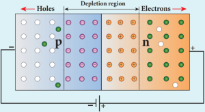
- As the positive potential is connected to the n-type material, the electrons in the n-type material are attracted towards the positive terminal in turn, the holes in the p-type material move towards the negative terminal (both away from the junction).
- It increases the immobile ions at the junction.
- The net effect is the widening of the depletion region.
- This leads to an increase in the barrier potential.
- Consequently, the majority charge carriers from both sides experience a great barrier to cross the junction.
- This reduces the diffusion current across the junction effectively.
- Yet, a small current flows across the junction due to the minority charge carriers in both regions.
- The reverse bias for majority charge carriers serves as the forward bias for minority charge carriers.
- The current that flows under a reverse bias is called the reverse saturation current.
- It is represented as Is
- The reverse saturation current is independent of the applied voltage and it depends only on the thermally generated minority charge carriers.
- Even a small voltage is sufficient enough to drive the minority charge carriers across the junction.
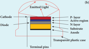
Light Emitting Diode (LED):
- LED is a p-n junction diode which emits visible or invisible light when it is forward biased.
- Since, electrical energy is converted into light energy, this process is also called electroluminescence.
- The circuit symbol of LED.
- The cross-sectional view of a commercial LED.
- It consists of a p-layer, n-layer and a substrate.
- A transparent window is used to allow light to travel in the desired direction.
- An external resistance in series with the biasing source is required to limit the forward current through the LED.
- In addition, it has two leads; anode and cathode.
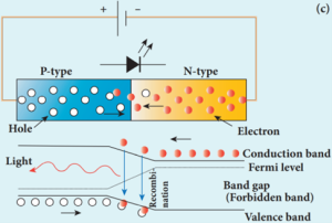
- When the p-n junction is forward biased, the conduction band electrons on n-side and valence band holes on p-side diffuse across the junction.
- When they cross the junction, they become excess minority carriers (electrons in p-side and holes in n-side).
- These excess minority carriers recombine with oppositely charged majority carriers in the respective regions, i.e. the electrons in the conduction band recombine with holes in the valence band.
- During recombination process, energy is released in the form of light (radiative) or heat (non-radiative).
- For radiative recombination, a photon of energy hv is emitted.
- For non-radiative recombination, energy is liberated in the form of heat.
- The colour of the light is determined by the energy band gap of the material.
- Therefore, LEDs are available in a wide range of colours such as blue (SiC), green (AlGaP) and red (GaAsP).
- Now a days, LED which emits white light (GaInN) is also available.
Applications:
- Indicator lamps on the front panel of the scientific and laboratory equipments.
- Seven-segment displays.
- Traffic signals, emergency vehicle lighting etc.
- Remote control of television, airconditioner etc.
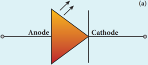
Photodiodes:
- A p-n junction diode which converts an optical signal into electric signal is known as photodiode.
- Thus, the operation of photodiode is exactly inverse to that of an LED. Photo diode works in reverse bias.
- Its circuit symbol.
- The direction of arrows indicates that the light is incident on the photo diode.
- The device consists of a p-n junction semiconductor made of photosensitive material kept safely inside a plastic case.
- It has a small transparent window that allows light to be incident on the p-n junction.
- Photodiodes can generate current when the p-n junction is exposed to light and hence are called as light sensors.
- When a photon of sufficient energy (hv) strikes the depletion region of the diode, some of the valence band electrons are elevated into conduction band, in turn holes are developed in the valence band.
- This creates electron-hole pairs.
- The amount of electron-hole pairs generated depends on the intensity of light incident on the p-n junction.
- These electrons and holes are swept across the p-n junction by the electric field created by reverse voltage before recombination takes place.
- Thus, holes move towards the n-side and electrons towards the p-side.
- When the external circuit is made, the electrons flow through the external circuit and constitute the photocurrent.
- When the incident light is zero, there exists a reverse current which is negligible.
- This reverse current in the absence of any incident light is called dark current and is due to the thermally generated minority carriers.
Applications:
- Alarm system
- Count items on a conveyer belt
- Photoconductors
- Compact disc players, smoke detectors
- Medical applications such as detectors for computed tomography etc.
Solar Cell:
- A solar cell, also known as photovoltaic cell, converts light energy directly into electricity or electric potential difference by photovoltaic effect.
- It is basically a p-n junction which generates emf when solar radiation falls on the p-n junction.
- A solar cell is of two types: p-type and n-type.
- Both types use a combination of p-type and n-type Silicon which together forms the p-n junction of the solar cell.
- The difference is that p-type solar cells use p-type Silicon as the base with an ultra-thin layer of n-type Silicon, while n-type solar cell uses the opposite combination.
- The other side of the p-Silicon is coated with metal which forms the back electrical contact.
- On top of the n-type Silicon, metal grid is deposited which acts as the front electrical contact.
- The top of the solar cell is coated with anti-reflection coating and toughened glass.
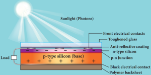
- In a solar cell, electron–hole pairs are generated due to the absorption of light near the junction.
- Then the charge carriers are separated due to the electric field of the depletion region.
- Electrons move towards n–type Silicon and holes move towards p-type Silicon layer.
- The electrons reaching the n-side are collected by the front contact and holes reaching p-side are collected by the back electrical contact.
- Thus a potential difference is developed across solar cell.
- When an external load is connected to the solar cell, photocurrent flows through the load.
- Many solar cells are connected together either in series or in parallel combination to form solar panel or module.
- Many solar panels are connected with each other to form solar arrays.
- For high power applications, solar panels and solar arrays are used.
Applications:
- Solar cells are widely used in calculators, watches, toys, portable power supplies, etc.
- Solar cells are used in satellites and space applications
- Solar panels are used to generate electricity.
The Bipolar Junction Transistor [BJT]:
Introduction:
- In 1951, William Schockley invented the modern version of transistor.
- It is a semiconductor device that led to a technological revolution in the twentieth century.
- The heat loss in transistor is very less.
- This has laid the foundation of integrated chips which contain thousands of miniaturized transistors.
- The emergence of the integrated chips led to increasing applications in the fast developing electronics industry.
Bipolar Junction Transistor:
- The BJT consists of a semiconductor (Silicon or Germanium) crystal in which an n-type material is sandwiched between two p-type materials (PNP transistor) or a p-type material sandwiched between two n-type materials (NPN transistor).
- To protect it against moisture, it is sealed inside a metal or a plastic case. The two types of transistors with their circuit symbols.
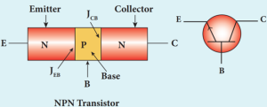
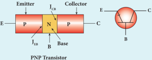
- The three regions formed are called as emitter, base and collector which are provided with terminals or ohmic contacts labeled as E, B, and C.
- As a BJT has two p-n junctions, two depletion layers are formed across the emitter-base junction (JEB) and collector-base junction (JCB) respectively.
- The circuit symbol carries an arrowhead at the emitter lead pointing from p to n indicating the direction of conventional current.
Emitter:
- The main function of the emitter is to supply majority charge carriers to the collector region through the base region.
- Hence, emitter is more heavily doped than the other two regions.
Base:
- Base is very thin (10-6m) and very lightly doped compared to the other two regions.
Collector:
- The main function of collector is to collect the majority charge carriers supplied by the emitter through the base.
- Hence, collector is made physically larger than the other two as it has to dissipate more power.
- Its is moderately dopped.
Transistor Biasing
- The application of suitable dc voltages across the transistor terminals is called biasing.
Different modes of transistor biasing:
Forward Active:
- In this bias the emitter-base junction is forward biased and the collector-base junction is reverse biased.
- The transistor is in the active mode of operation.
- In this mode, the transistor functions as an amplifier.
Saturation:
- Here, the emitter-base junction and collector-base junction are forward biased.
- The transistor has a very large flow of currents across the junctions.
- In this mode, transistor is used as a closed switch.
Cut-off:
- In this bias, the emitter-base junction and collector-base junction are reverse biased.
- Transistor in this mode is an open switch.
Integrated Chips:
- An integrated circuit is also referred as an IC or a chip or a microchip.
- It consists of thousands to millions of transistors, resistors, capacitors, etc. integrated on a small flat piece of semiconductor material that is normally Silicon.
- Integrated circuits (ICs) are the keystone of modern electronics.
- With the advancement in technology and the emergence of Very Large Scale Integration (VLSI) era it is possible to fit more and more transistors on chips of same piece.
- ICs have two main advantages over ordinary circuits: cost and performance.
- The size, speed, and capacity of chips have progressed enormously with the advancement in technology.
- Computers, mobile phones, and other digital home appliances are now made possible by the small size and low cost of ICs. ICs can function as an amplifier, oscillator, timer, micro processor and computer memory.
- These extremely small ICs can perform calculations and store data using either digital or analog technology.
- Digital ICs use logic gates, which work only with values of ones and zeros.
- A low signal sent to a component on a digital IC will result in a value of 0, while a high signal creates a value of 1.
- Digital ICs usually find their applications in computers, networking equipment, and most consumer electronics.
- Analog ICs or linear ICs work with continuous values.
- This means a component on a linear IC can take any value and output another value.
- Linear ICs are typically used in audio and radio frequency amplification.
Propagation of Electromagnetic Waves:
- The information signal modulated with the carrier wave (radio wave) is transmitted by an antenna.
- This travels through space and is received by the receiving antenna at the other end.
- The frequencies from 2 kHz to 400 GHz are transmitted through wireless communication.
- The strength of the electromagnetic wave keeps decreasing while traveling from transmitter to the receiver.
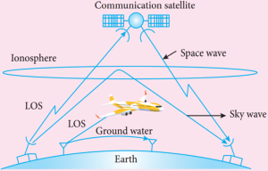
- The electromagnetic wave transmitted by the transmitter travels in three different modes to reach the receiver according to its frequency range:
- Ground wave propagation (or) surface wave propagation (nearly 2 kHz to 2 MHz)
- Sky wave propagation (or) ionospheric propagation (nearly 3 MHz to 30 MHz)
- Space wave propagation (nearly 30 MHz to 400 GHz)
Ground Wave Propagation:
- If the electromagnetic waves transmitted by the transmitter glide over the surface of the earth to reach the receiver, then the propagation is called ground wave propagation.
- The corresponding waves are called ground waves or surface waves.
- Both transmitting and receiving antennas must be close to the earth.
- The size of the antenna plays a major role in deciding the efficiency of the radiation of signals.
- During transmission, the electrical signals are attenuated over a distance. Some reasons for attenuation are as follows:
- Increasing distance: The attenuation of the signal with distance depends on
- power of the transmitter
- frequency of the transmitter and
- condition of the Earth surface.
- Absorption of energy by the Earth:
- When the transmitted signal in the form of EM wave is in contact with the Earth, it induces charges in the Earth and constitutes a current.
- Due to this, the Earth behaves like a leaky capacitor which leads to the attenuation of the wave.
- Tilting of the wave:
- As the wave progresses, the wavefront starts gradually tilting according to the curvature of the Earth.
- This increase in the tilt decreases the electric field strength of the wave.
- Finally at some distance, the surface wave dies out due to energy loss.
- The frequency of the ground waves is mostly less than 2 MHz as high frequency waves undergo more absorption of energy at the earth’s atmosphere.
- The medium wave signals received during the day time use surface wave propagation.
- It is mainly used in local broadcasting, radio navigation, for ship-to-ship, shipto-shore communication and mobile communication.
Sky Wave Propagation:
- The mode of propagation in which the electromagnetic waves radiated from an antenna, directed upwards at large angles, gets reflected by the ionosphere back to earth is called sky wave propagation or ionospheric propagation.
- The corresponding waves are called sky waves.
- The frequency range of EM waves in this mode of propagation is 3 to 30 MHz. EM waves of frequency more than 30 MHz can easily penetrate through the ionosphere and does not undergo reflection.
- It is used for short wave broadcast services.
- Medium and high frequencies are for long-distance radio communication.
- Extremely long-distance communication is also possible as the radio waves can undergo multiple reflections between the earth and the ionosphere.
- A single reflection helps the radio waves to travel a distance of approximately 4000 km.
- Ionosphere acts as a reflecting surface.
- It is at a distance of approximately 50 km and spreads up to 400 km above the Earth surface.
- Due to the absorption of ultraviolet rays, cosmic ray, and other high energy radiations like α, β rays from sun, the air molecules in the ionosphere get ionized.
- This produces charged ions and these ions provide a reflecting medium for the reflection of radio waves or communication waves back to Earth within the permitted frequency range.
- The phenomenon of bending the radio waves back to earth is nothing but the total internal reflection.
- This is the reason why the EM waves are transmitted at a critical angle to ensure that the waves undergo total reflection and reaches the ground without escaping into space.
- The shortest distance between the transmitter and the point of reception of the sky wave along the surface is called as the skip distance.
- The electromagnetic waves are transmitted from the ground at particular angles.
- When the angle of emission increases, the reception of ground waves decreases.
- At one point, there will be no reception due to ground waves and marked as A.
- If the angle of emission is increased further, the reception of sky waves starts at point B.
- There is a zone (in between A and B) where there is no reception of electromagnetic waves neither ground nor sky, called as skip zone or skip area.
Space Wave Propagation:
- The process of sending and receiving information signal through space is called space wave communication.
- The electromagnetic waves of very high frequencies above 30 MHz are called as space waves.
- These waves travel in a straight line from the transmitter to the receiver.
- Hence, it is used for a line of sight communication (LOS).
- For high frequencies, the transmission towers must be high enough so that the transmitted and received signals (direct waves) will not encounter the curvature of the Earth and hence travel with less attenuation and loss of signal strength.
- Certain waves reach the receiver after getting reflected from the ground.
- The communication systems like television telecast, satellite communication and RADAR are based on space wave propagation.
- Microwaves having high frequencies (super high frequency band) are used against radio waves due to certain advantages: larger bandwidth, high data rates, better directivity, small antenna size, low power consumption, etc.
- The range or distance (d) of coverage of the propagation depends on the height (h) of the antenna given by the equation,
- Where R is the radius of the Earth and it is 6400 km.
Satellite Communication:
- The satellite communication is a mode of communication of signal between transmitter and receiver via satellite.
- The message signal from the Earth station is transmitted to the satellite on board via an uplink (frequency band 6 GHz), amplified by a transponder and then retransmitted to another Earth station via a downlink (frequency band 4 GHz).
- The high-frequency radio wave signals travel in a straight line (line of sight) may come across tall buildings or mountains or even encounter the curvature of the earth.
- A communication satellite relays and amplifies such radio signals via transponder to reach distant and far off places using uplinks and downlinks.
- It is also called as a radio repeater in sky.
Applications:
- Satellites are classified into different types based on their applications. Some satellites are discussed below.
- Weather Satellites: They are used to monitor the weather and climate of Earth. By measuring cloud mass, these satellites enable us to predict rain and dangerous storms like hurricanes, cyclones etc.
- Communication satellites: They are used to transmit television, radio, internet signals etc. Multiple satellites are used for long distances.
- Navigation satellites: These are employed to determine the geographic location of ships, aircrafts or any other object.
Fibre Optic Communication:
- The method of transmitting information from one place to another in terms of light pulses through an optical fiber is called fiber optic communication.
- It works under the principle of total internal reflection.
- Light has very high frequency (400 THz – 790 THz) than microwave radio systems.
- The fibers are made up of silica glass or silicon dioxide which is highly abundant on Earth.
- Now it has been replaced with materials such as chalcogenide glasses, fluoroaluminate crystalline materials because they provide larger infrared wavelength and better transmission capability.
- As fibers are not electrically conductive, it is preferred in places where multiple channels are to be laid and isolation is required from electrical and electromagnetic interference.
Applications:
- Optical fiber system has a number of applications namely, international communication, inter-city communication, data links, plant and traffic control and defense applications.
Merits:
- Fiber cables are very thin and weigh lesser than copper cables.
- This system has much larger band width.
- This means that its information carrying capacity is larger.
- Fiber optic system is immune to electrical interferences.
- Fiber optic cables are cheaper than copper cables.
Demerits:
- Fiber optic cables are more fragile when compared to copper wires.
- It is an expensive technology.
Radar and Applications:
- Radar basically stands for Radio Detection and Ranging System.
- It is one of the important applications of communication systems and is mainly used to sense, detect, and locate distant objects like aircraft, ships, spacecraft, etc.
- The angle, range or velocity of the objects that are invisible to the human eye can be determined.
- Radar uses electromagnetic waves for communication.
- The electromagnetic signal is initially radiated into space by an antenna in all directions.
- When this signal strikes the targeted object, it gets reflected or reradiated in many directions.
- This reflected (echo) signal is received by the radar antenna which in turn is delivered to the receiver.
- Then, it is processed and amplified to determine the geographical statistics of the object.
- The range is determined by calculating the time taken by the signal to travel from RADAR to the target and back.
Applications:
- Radars find extensive applications in almost all fields. A few are mentioned below.
- In military, it is used for locating and detecting the targets.
- It is used in navigation systems such as ship borne surface search, air search and missile guidance systems.
- To measure precipitation rate and wind speed in meteorological observations, Radars are used.
- It is employed to locate and rescue people in emergency situations.
Mobile Communication:
- Mobile communication is used to communicate with others in different locations without the use of any physical connection like wires or cables.
- It allows the transmission over a wide range of area without the use of the physical link.
- It enables the people to communicate with each other regardless of a particular location like office, house etc.
- It also provides communication access to remote areas.
- It provides the facility of roaming – that is, the user may move from one place to another without the need of compromising on the communication.
- The maintenance and cost of installation of this communication network are also cheap.
Applications:
- It is used for personal communication and cellular phones offer voice and data connectivity with high speed.
- Transmission of news across the globe is done within a few seconds.
- Using Internet of Things (IoT), it is made possible to control various devices from a single device. Example: home automation using a mobile phone.
- It enables smart classrooms, online availability of notes, monitoring student activities etc. in the field of education.
Application of Information and Communication Technology in Agriculture, Fisheries and Mining:
Agriculture:
- The implementation of information and communication technology (ICT) in agriculture sector enhances the productivity, improves the living standards of farmers and overcomes the challenges and risk factors.
- ICT is widely used in increasing food productivity and farm management.
- It helps to optimize the use of water, seeds and fertilizers etc.
- Sophisticated technologies that include robots, temperature and moisture sensors, aerial images, and GPS technology can be used.
- Geographic information systems are extensively used in farming to decide the suitable place for the species to be planted.
Fisheries:
- Satellite vessel monitoring system helps to identify fishing zones.
- Use of barcodes helps to identify time and date of catch, species name, quality of fish.
Mining:
- ICT in mining improves operational efficiency, remote monitoring and disaster locating system.
- Information and communication technology provides audio-visual warning to the trapped underground miners.
- It helps to connect remote sites.